
FPGA Design Flow
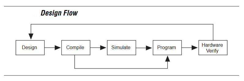
The standard FPGA design flow starts with design entry using schematics or a hardware description language (HDL), such as Verilog HDL or VHDL. In this step, you create the digital circuit that is implemented inside the FPGA. The flow then proceeds through compilation, simulation, programming, and verification in the FPGA hardware
To get started with FPGA programming, you need to have a good background in digital logic design in order to get familiar with logic values, logic gates, combinational and sequential logic circuits. This is a good resource for it.
This article does not explain the basic concepts of programmable logic.
- You are somewhat familiar with digital circuit design and electronic design automation (EDA) tools.
- You have installed the Altera® Quartus® II software on your computer. If you do not have the Quartus II software, you can download it from the Altera web site at www.altera.com/download.
- You have an Altera Cyclone® III, Stratix® III, or ArriaTM GX Development Board (or equivalent) on which you will test your project. Using a development board helps you to verify whether your design is really working.
- You have gone through the quick start guide and/or the getting started user guide for your development kit. These documents ensure that you have:
- Installed the required software.
- Determined that the development board functions properly and is connected to your computer.●Installed the USB-Blaster™ driver, which allows you to program the FPGA on the development board with your own design.
- Verilog/ VHDL language – Then, you can start studying Verilog/ VHDL for programming FPGAs. Verilog/ VHDL is the hardware description language
- Simulation -To practice FPGA programming, simulation is a critical step before synthesis and implementation. Simulation is to verify the functional correctness of the Verilog/ VHDL code that you write.
- Synthesis and Implementation – After successfully verified the design in functional simulation, you can think about the next step of synthesis and Implementation. The two most popular synthesis and implementation tools for FPGAs are Xilinx ISE/ Vivado Design suite for Xilinx FPGAs and Quartus II for Intel Altera FPGAs. It is also noted that you can simulate your design with these tools; simulators (Xilinx ISIM, ModelSim-Altera) are integrated into Xilinx ISE/ Quartus II. The tool enables synthesizing code and generating the bit stream file for FPGA programming.
- FPGA Development Boards – After obtained the bitstream file from Xilinx ISE/ Vivado/ Quartus II, we will download the bitstream to FPGA boards for demonstrations.
I will recommend FPGA board for beginner